Products
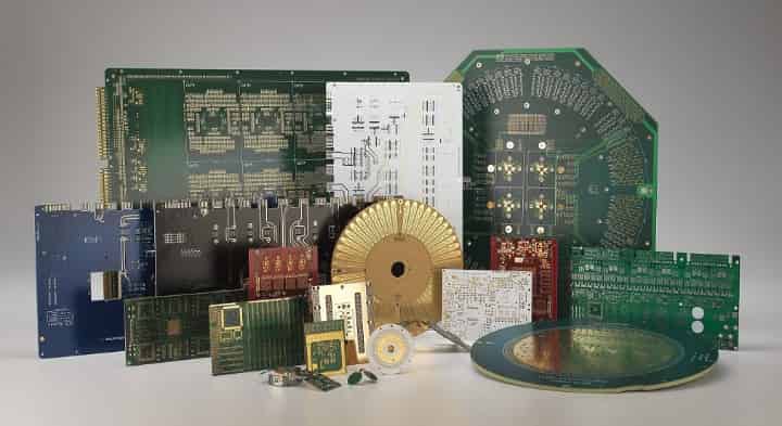
The fima's production goes from D/F up to
40-layer PCBs. The technology involved in FIMA covers a
wide range of products. Flex and rigid-flex PCBs, HDI PCBs, RF PCBs, and more.
The high level
of our
technology includes copper via filling, vias filled and resin filled, laser microvias, and SBU
technology.
Special Products
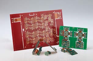
Flex and Rigid-Flex PCBs
Typically used in avionics and military applications, FIMA is able to supply flexible single-sided, double-sided, multilayer, and multilayer rigid-flex circuits with two or more different flexible layers, blind vias, and all surface finishings.
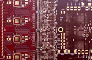
HDI PCBs
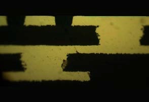
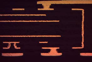
FIMA can produce printed circuit boards with very dense interconnections (HDI), very fine lines, and very small gaps (down to 25 μm). Usually these PCBs have buried vias and simple, staggered, stacked blind microvias over several levels; the production of HDI boards is made easy by the use of laser technology. Available surface finishes on these PCBs are ENIG, ENEPIG, and Immersion Tin.
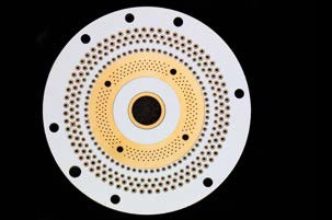
RF PCBs
These PCBs are designed for high-frequency applications and are produced using special laminates, often a mix of different materials. RF PCBs need dimensional checks of the pattern through an automatic optical inspection (AOI) machine. The impedance values of the signal lines have to be certified through coupons and measurement protocols.
Leading Edge Processing
Copper Via Filling
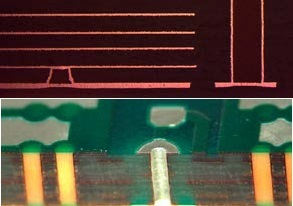
Two lines dedicated to copper filling of blind vias are available at FIMA: the first one is a standalone line, and the second one is integrated into the plating line for panel plating. This process is expressly required for HDI boards where vias in pad holes are present. The highest depth of the dimple is guaranteed to be lower than 5 μm.
Vias Filled & Capped and Resin Filled
The Filled & Capped process is meant to fill blind vias or PTH holes with resin and plate their top and bottom. The resulting cylinder allows soldering or electrical or mechanical contact. This process is carried out by a machine, which fills the holes with epoxy resin. The excess resin is removed by a plane razing machine to achieve a clean and uniform surface. The dimple depth is, in practice, absent. The same machine is also used to selectively fill PTH holes with resin after etching.
Laser Microvias and SBU Technology
SBU (Sequential Build Up) technology is used for HDI circuits requiring several lamination and drilling levels: drill sizes down to 50 μm, track and gap widths down to 25 μm are their main features. This technology is available at FIMA and is performed by LDI machines to print inner layers, outer layers, and solder masks, while the laser drilling machine is used to drill the blind microvias.